Page 67 - Plastics News January 2023
P. 67
TECHNOLOGY


          3D Printing Method Fabricates Complex Metal Plastic Composite Struc-
          tures
                                                                                 Such 3D metal–plastic composite
                                                                                 structures have widespread potential
                                                                                 applicability in smart electronics, mi-
                                                                                 cro/nanosensing,  internet-of-things
                                                                                 (IoT) devices, and even  quantum
                                                                                 computing, according to the research-
                                                                                 ers. 3D printing these structures gives
                                                                                 the devices they’re put into a higher
                                                                                 degree of  design freedom, with the
                                                                                 possibility  more  complex  features
                                                                                 and geometry, as well as increasingly
                                                                                 smaller sizes. They have not been
                                                                                 widely  adopted,  however,  because
                                                                                 the current methods to fabricate such
                                                                                 parts are expensive and complicated.
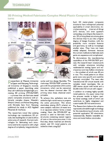
                                                                                 To demonstrate the manufacturing
                                                                                 capabilities of the MM-DLP3DP pro-
                                                                                 cess, the research team created parts
                                                                                 with complex structures  including
                                                                                 multimaterial  nesting  layers  and mi-
                                                                                 croporous and tiny hollow structures
                                                                                 — the smallest of which was 40 µm
                                                                                 in size. The metal patterns on these
                                                                                 parts were very specific and could be
                                                                                 precisely controlled. The team also
             esearchers  at Waseda University  cycles and low-design flexibility. The   manufactured 3D circuit boards with
          Rof Japan and Nanyang Technologi-   multi-step MM-DLP3DP process be-   complex metal topologies,  like  an
          cal University of  Singapore recently  gins with the preparation of the active   LED stereo circuit with nickel and a
          published a paper describing what  precursors, which can be converted   double-sided 3D circuit with copper.
          they call multimaterial digital light pro-  into the desired chemical after 3D   In addition to creating highly specific
          cessing  3D printing  (MM-DLP3DP)  printing since these chemical aren’t   metal patterns, the paper notes that
          — a process that can fabricate metal  printable.                       the process results in higher qual-
          plastic composite structures with ar-  To achieve  this,  palladium ions are   ity metal coatings, both of which can
          bitrarily complex shapes. Waseda’s  added to light-cured resins to prepare   contribute  to highly  integrated  and
          Shinjiro Umezu and Kewei Song along  the  active  precursors.  This  allows   customizable 3D microelectronics.
          with Hirotaka Sato from  Nanyang  electroless  plating  (ELP)  wherein  an
          published the study in ACS Applied  auto-catalytic reduction of metal ions   The Researchers believe this advance
          Materials & Interfaces.             in an aqueous solution forms a metal   represents a breakthrough technology
                                                                                 for the manufacturing of circuits, with
          The researchers noted that existing   coating. Next, the  MM-DL3DP ap-  potential  application 3D electronics,
          technology  can manufacture 3D cir-  paratus is  used  to  fabricate  micro-  metamaterials,  flexible  wearable  de-
          cuits, but stacking flat circuits Is still an   structures  containing nested  regions   vices and metal hollow electrodes.
          active area of research. Current tech-  of resin or the active precursor. In the
          nologies for fabricating  such struc-  final step, these materials are directly
          tures tend to be expensive with a high   plated, and 3D metal patterns are
          degree of complexity, long production   added to them using ELP.


          January 2023                                                                           PLASTICS NEWS 67

